- 您现在的位置:买卖IC网 > Sheet目录1994 > DS3232SN#T&R (Maxim Integrated Products)IC RTC W/TCXO 20-SOIC
Extremely Accurate I2C RTC with
Integrated Crystal and SRAM
ABSOLUTE MAXIMUM RATINGS
RECOMMENDED OPERATING CONDITIONS
(TA = -40°C to +85°C, unless otherwise noted.) (Notes 2, 3)
Stresses beyond those listed under “Absolute Maximum Ratings” may cause permanent damage to the device. These are stress ratings only, and functional
operation of the device at these or any other conditions beyond those indicated in the operational sections of the specifications is not implied. Exposure to
absolute maximum rating conditions for extended periods may affect device reliability.
Voltage Range on VCC, VBAT, 32kHz, SCL, SDA, RST,
INT/SQW Relative to Ground.............................-0.3V to +6.0V
Junction-to-Ambient Thermal Resistance (
θJC) (Note 1)..55.1°C/W
Junction-to-Case Thermal Resistance (
θJC) (Note 1)..........24°C/W
Operating Temperature Range
(noncondensing) .............................................-40°C to +85°C
Junction Temperature ......................................................+125°C
Storage Temperature Range ...............................-40°C to +85°C
Lead Temperature (soldering, 10s) .................................+260°C
Soldering Temperature (reflow, 2 times max) ....................+260°C
(See the
Handling, PC Board Layout, and Assembly section.)
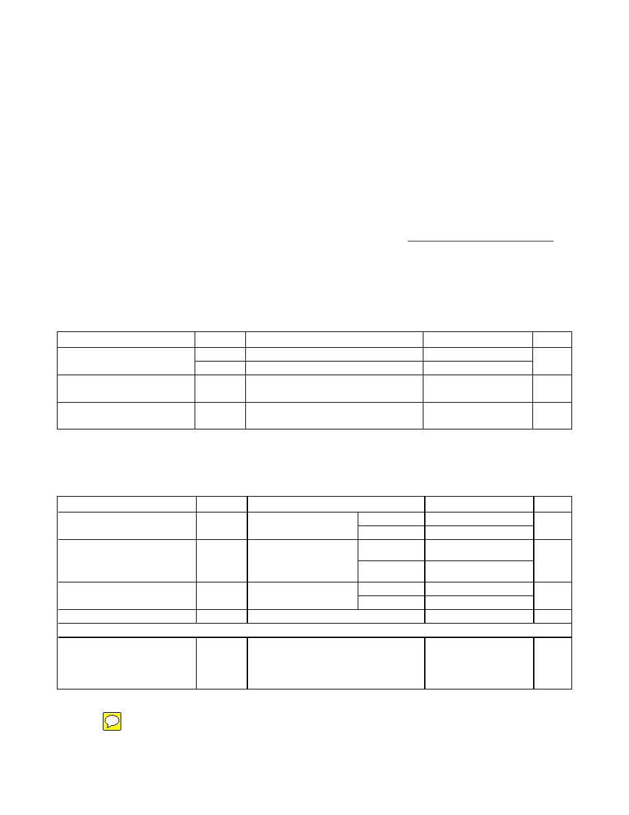
PARAMETER
SYMBOL
CONDITIONS
MIN
TYP
MAX
UNITS
VCC
2.3
3.3
5.5
Supply Voltage
VBAT
2.3
3.0
5.5
V
Logic 1 Input SDA, SCL
VIH
0.7 x
VCC
VCC +
0.3
V
Logic 0 Input SDA, SCL
VIL
-0.3
+0.3 x
VCC
V
ELECTRICAL CHARACTERISTICS
(VCC = 2.3V to 5.5V, VCC = active supply (see Table 1), TA = -40°C to +85°C, unless otherwise noted.) (Typical values are at VCC =
3.3V, VBAT = 3.0V, and TA = +25°C, unless otherwise noted.) (Notes 2, 3)
PARAMETER
SYMBOL
CONDITIONS
MIN
TYP
MAX
UNITS
VCC = 3.3V
200
Active Supply Current
ICCA
32kHz output off
(Notes 4, 5)
VCC = 5.5V
325
A
VCC = 3.3V
120
Standby Supply Current
ICCS
I2C bus inactive, 32kHz
output off, SQW output off
(Note 5)
VCC = 5.5V
160
A
VCC = 3.3V
500
Temperature Conversion Current
ICCSCONV
I2C bus inactive, 32kHz
output off, SQW output off
VCC = 5.5V
600
A
Power-Fail Voltage
VPF
2.45
2.575
2.70
V
ACTIVE SUPPLY (Table 1 ) (2.3V to 5.5V, TA = -40°C to +85°C, unless otherwise noted) (Note 2)
Logic 1 Output, 32kHz
IOH = -1mA
IOH = -0.75mA
IOH = -0.14mA
VOH
Active supply > 3.3V,
3.3V > active supply > 2.7V,
2.7V > active supply > 2.3V
2.0
V
Note 1: Package thermal resistances were obtained using the method described in JEDEC specification JESD51-7, using a four-
layer board. For detailed information on package thermal considerations, refer to www.maxim-ic.com/thermal-tutorial.
DS3232
2
Maxim Integrated
发布紧急采购,3分钟左右您将得到回复。
相关PDF资料
DS3234S#
IC RTC W/TCXO 20-SOIC
DS32C35-33#T&R
IC RTC ACCURATE I2C 3.3V 20-SOIC
DS3911T+
IC DAC 10BIT I2C QUAD 14TDFN
DS4000KI/WBGA
IC OSC TCXO 19.44MHZ 24-BGA
DS4026S+WCN
IC OSC TCXO 25MHZ 16-SOIC
DS4100HW+
IC OSC CLOCK 100MHZ 10LCCC
DS4266P+
IC OSC CLOCK 266MHZ 10-LCCC
DS4302Z-020/T&R
IC DAC 5-BIT SGL 0-2.0V 8-SOIC
相关代理商/技术参数
DS3232SN#-W
功能描述:实时时钟 RoHS:否 制造商:Microchip Technology 功能:Clock, Calendar. Alarm RTC 总线接口:I2C 日期格式:DW:DM:M:Y 时间格式:HH:MM:SS RTC 存储容量:64 B 电源电压-最大:5.5 V 电源电压-最小:1.8 V 最大工作温度:+ 85 C 最小工作温度: 安装风格:Through Hole 封装 / 箱体:PDIP-8 封装:Tube
DS3234
制造商:MAXIM 制造商全称:Maxim Integrated Products 功能描述:Extremely Accurate SPI Bus RTC with Integrated Crystal and SRAM
DS3234_07
制造商:MAXIM 制造商全称:Maxim Integrated Products 功能描述:Extremely Accurate SPI Bus RTC with Integrated Crystal and SRAM
DS3234_08
制造商:MAXIM 制造商全称:Maxim Integrated Products 功能描述:Extremely Accurate SPI Bus RTC with Integrated Crystal and SRAM
DS3234_10
制造商:MAXIM 制造商全称:Maxim Integrated Products 功能描述:Extremely Accurate SPI Bus RTC with Integrated Crystal and SRAM
DS3234_BREAKOUT_
制造商:MCM 功能描述:DS3234 BREAKOUT BOARD 制造商:PREMIER FARNELL 功能描述:DS3234 BREAKOUT BOARD
DS3234_BREAKOUT_B34
制造商:Distributed By MCM 功能描述:DS3234 Real Time Clock Breakout Board
DS3234S
制造商:MAXIM 制造商全称:Maxim Integrated Products 功能描述:Extremely Accurate SPI Bus RTC with Integrated Crystal and SRAM